

Latest Customer Satisfied Contract Manufacturing Electronics
-
Price:
Negotiable
- minimum:
- Total supply:
-
Delivery term:
The date of payment from buyers deliver within days
-
seat:
Guangdong
-
Validity to:
Long-term effective
-
Last update:
2017-11-27 01:39
-
Browse the number:
204
+
Guangzhou NOD Electronics Co., Ltd.
- Contactaixin:
Mr. Rocky Long(Mr.)
-
Email:
telephone:
phone:

-
Arrea:
Guangdong
Address:Block3, #20-8, Huanxi West Rd, Tianhe District, Guangzhou, Guangdong, China 510660
- Website:
+
Latest Customer Satisfied Contract Manufacturing Electronics
About Us
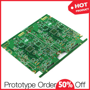
As a service-leading PCB manufacturing and PCB assembly (PCBA) partner, NOD Electronics strives to support international small-medium business with 10+ years engineering experience in Electronic Manufacturing Services (EMS). Our headquarter is located in Guangzhou, China. We have 10,000 square meters plant, 287 employees and 42 engineers, monthly capabilities of 15,000 square meters PCB design & fabrication and 80 million spot SMT. We were approved by ISO9001-2008, TS16949, UL, CE, RoHS.

NOD Contract Manufacturing Electronics Capabilities
| Total Pad Size | Standard | Advanced |
| Capture Pad | Drill + 0.008 | Drill + 0.006 |
| Landing Pad | Drill + 0.008 | Drill + 0.006 |
| BC Mechanical Drill (Type III) | 0.008 | 0.006 |
| Laser Drill Size | 0.004-0.010 | 0.0025 |
| Material Thickness | 0.0035 | 0.0025 |
| Stacked Via | Yes | Yes |
| Type I Capabilities single & Double Deep | Yes | Yes |
| Type II Capabilities Buried Vias with Microvias | Yes | Yes |
| Type III Capabilities | Yes | Yes |
| Copper Filled Microvia | Yes | Yes |
| Smallest Copper Filled Microvia | 0.004 | 0.0025 |
| Copper Filled Microvia Aspect Ratio | 0.75:1 | 1:01 |
| Smallest Laser Microvia Hole Size | 0.004 | 0.0025 |
| Laser Via Aspect Ratio (Depth:Diameter) | 0.75:1 | c |
NOD Contract Manufacturing Electronics Process

We are offering PCB/PCBA electronics manufacturing and assembly services to following big customers all over the world

Your PCB /PCBA electronics demand will be perfectly handled by our professional production line and responsible work team.

Frequently Asked Questions (FAQs)
How we ensure the quality of contract manufacturing electronics ?
We choose top sheet suppliers to ensure stable performance (general FR-4). During the manufacturing process, automatic copper plating lines and high-speed drilling machines (brand:TMAX) to make accuracy and fast delivery guaranteed. All printed circuit board will be detected by advanced automatic flying probe machines (or test frame ) at subsequent stages to make sure each PCB is OK from inner circuits to outside shape.
How long will you get our quotation of PCB/PCBA?
In general, PCB sample is delivered in 24~72 hours (urgent order less than 24 hours). Volume production can be completed in 7 working days. If for subsequent PCB assembly and test requirements, the lead time could be less than 15 days.
What kind of files you have to send us to get quotation?
You have to send us PCB design files (gerbers or .pcb acceptable), Bill of Materials (BOM), Quantities to make quote and other technical requirements (.step/.txt/.xls files acceptable)
What payment methods we can support?
We accept T/T, L/C, West Union as payment methods. For prototype order, you have to make 100% payment in advance, but for mass production 70% payment in advance and 30% payment before delivery.
What measures we take to avoid counterfeit components?
Procurement only from manufacturer or big general agent
Original quality certificate of component can be issued (if necessary)
Inspections of shape, silkscreen and conductivity attributes in incoming quality control
Strong responsibilities and perspectives of long-term relationship
What measures we take to protect clients IP and confidentiality?
Sign NDA (Non-disclosure Agreement)
Using number code in stead of client name during manufacturing process
Separate assembly workshop and taking photo is NOT allowed
Documents of engineering process are archived and reserved
other products

